.svg "bes-logo (1)")
Realizing PCB Silkscreen’s Full Potential
Realizing PCB Silkscreen’s Full Potential
I have seen many approaches to PCB Silkscreen over the years. Some PCB silkscreen facilitates incoming inspection and provides useful information to test and assembly personnel. Other PCB silkscreen offers little added value and in some instances can even reduce reliability! I think the most important things that a PCB Designer can consider when designing silkscreen are “Who are my stakeholders?” and “How can I support them with my silkscreen design?”. With those two questions answered, your PCB Silkscreen design is sure to realize its full potential!
PCB Silkscreen should be seen, not hidden!
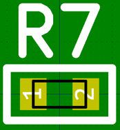
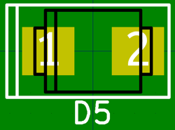
Boulder Engineering Studio resistor silkscreen design |
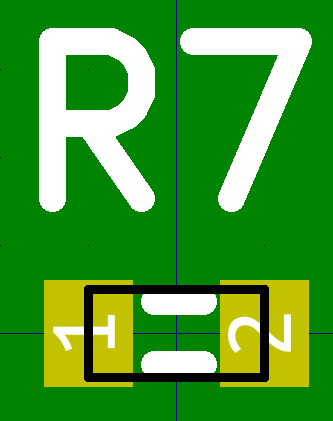
Not recommended: Silkscreen under resistor could cause defects at reflow |
One of the most common issues that I see is PCB silkscreen underneath components. This is due to the PCB designer creating the silkscreen for one stakeholder only: component placement personnel. There are several issues with this approach:
1. Most PCBs will have component placement performed by pick-and-place machines and not humans. Pick-and-place machines locate components based on a precision copper fiducial pattern on the PCB and a component origin file exported from the master layout, not PCB silkscreen.
2. This approach does not take into account all of the post-assembly personnel that could benefit from viewing the PCB silkscreen during inspection, rework, repair, bring-up and troubleshooting such as quality inspectors, soldering technicians and electrical engineers.
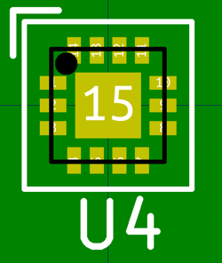 Boulder Engineering Studio QFN silkscreen design Boulder Engineering Studio QFN silkscreen design |
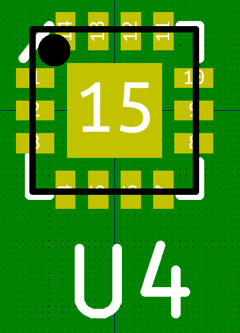 Not recommended: Silkscreen under QFN body may cause soldering defects and QFN is difficult to rework Not recommended: Silkscreen under QFN body may cause soldering defects and QFN is difficult to rework |
3. Lastly, and most risky, is that PCB silkscreen under small, flush-mount components can actually increase ppm defects in volume assembly leading to increased scrap and decreased profits! Silkscreen does have a z-axis profile and a registration tolerance. When placed under or nearly under an 0201 or 0402 resistor or capacitor or a flush-mount DFN, QFN or LGA, it can actually bump up the component during reflow causing costly soldering defects.
Boulder Engineering Studio diode silkscreen design |
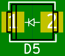
Not recommended: Diode polarity is not visible after component is installed |
In order to realize its full potential, PCB silkscreen must not be hidden under components.
PCB Silkscreen can support many user functions!
PCB Silkscreen can be more than just reference designators for component installation and inspection. It can also support other functions such as circuit debug, user interface and final product assembly. Some examples of enhanced use of PCB silkscreen are: 1. PCB Silkscreen can be used to mark net names at test points, connectors and other access points to facilitate bring-up and circuit debug for hardware engineers. It can also be used to define LEDs and buttons. 2. PCB Silkscreen can be used to support field installation of the hardware such as marking wire colors or wire routing next to a terminal block. 3. PCB Silkscreen can also be used to facilitate product assembly such as marking battery polarities, adhesive application zones or label locations.
It is important that PCB Designers consider all of the possible PCB Silkscreen stakeholders in order to realize its full potential.
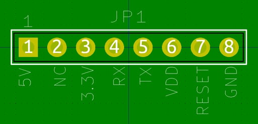
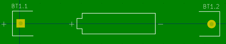
Net names are marked on header pins for debug |
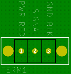
Signal names and installation direction marked on Terminal Block |
|
Component placement is marked for soldering- Battery orientation is marked for final assembly |
||
At Boulder Engineering Studio, our PCB Design Team understands the full potential of PCB Silkscreen and we apply this understanding to each PCB Design from Prototyping to Finalization to Production.