.svg "bes-logo (1)")
Design
Why Manual Visual Inspection is a Vital Method of Defect Detection
Why Manual Visual Inspection is a Vital Method of Defect Detection
Manual visual inspection is an important part of our process at BES. We visually inspect every new run of boards that we order from any manufacturer, regardless of whether we order from a new vendor or from one well known to BES. We evaluate everything on the board, from solder mask to solder joints. We even evaluate shipping packaging. As we refine our designs, manual visual inspection continues to be useful throughout the process, from prototyping to large-scale manufacturing. It is the first step for us to identify design or manufacturing issues, and we have found it to be valuable and worth repeating.
Why is manual visual inspection important?
Even with more sophisticated, automated optical inspection methods available from many PCBA manufacturers, visual inspection by skilled personnel remains a relevant method to find problems. Even when other inspection processes are omitted, manufacturers will still include manual visual inspection at key points in their process.[1]
The majority of defects in the PCBA assembly process are structural in nature. As shown in the chart below, missing electrical components, misalignment, incorrect orientation, insufficient/excess solder, and shorts make up a large portion of PCBA manufacturing defects, many of which will be readily visible to a skilled observer.
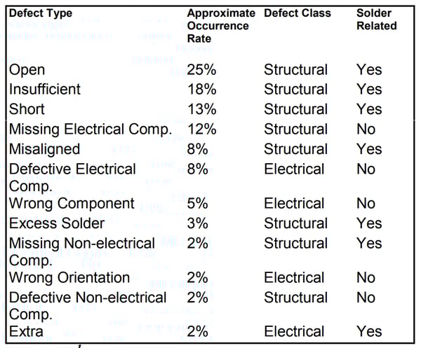
Industry data for the incidence rates of common PCB defects, many of which are structural in nature and can be found with manual visual inspection.[2]
How does MVI benefit our process at BES?
Manual visual inspection is an especially important step for us when we are evaluating early revision PCBA designs. It helps filter out damaged or poorly processed boards from our testing pool. In these early stages, we need to be focused on both testing the design and validating the board house’s process. Identifying issues related to manufacturing defects or poor processing as early as possible can save significant time and effort in the testing and PCBA debugging process.
Findings from manual inspection allow us to evaluate the board houses themselves. Shown is an image of a prototype board that we ordered from a board house that we were trying out for the first time. When we received the boards, the solder mask had some unusual damage, as shown in the image below. Upon investigation, we learned that when we ordered a finish that the board house did not carry, they had used a normal solder mask and had buffed the finish to the matte we ordered. While it is hard to anticipate a deviation such as this, adding specific language to request approval for changes to process can help instill a better level of communication.
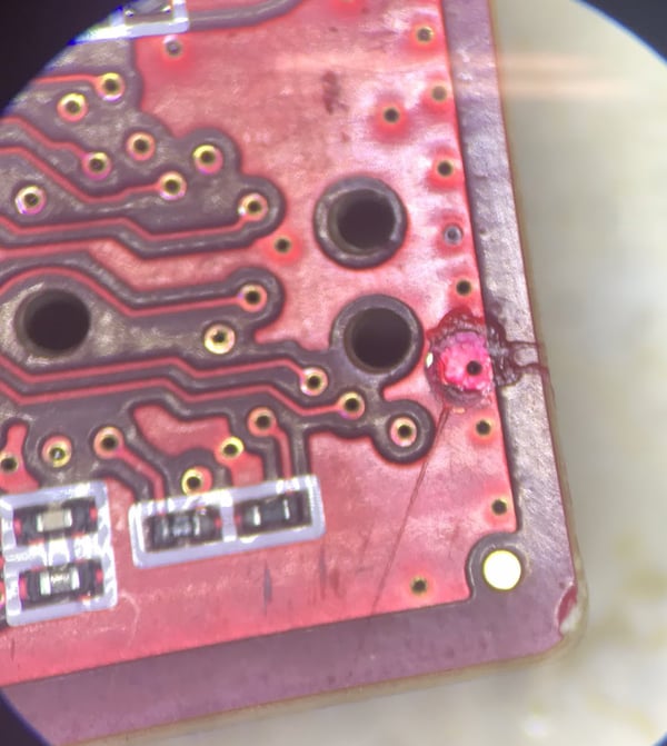
Process indicators and damage to a board that was buffed to achieve a matte finish on the solder mask.
As designs are refined later in development, visual inspection continues to be useful. We often order several small early runs from a board house during prototyping, and each board spin is an opportunity for refinement. Visual inspection can reveal problems with land patterns. It also allows us to evaluate certain design choices and make changes. As we go through iterations of board design, we consistently look for process indicators and defects, which helps us refine and document the manufacturing process. This is very much a collaborative effort between the designer and the manufacturer. The more feedback that can be provided is generally the better to achieve a design that is easy to manufacture consistently.
In early stages of development, we inspect each board in initial small prototyping runs. This will often be on the order of 5-50 PCBAs. Though it may require a significant amount of a technician’s time to inspect a larger number of boards, the sooner we can catch problems, the easier (and cheaper) the manufacturing process will be in later stages. We can find and flag problem areas before they become magnified by larger-volume production.
Once the PCBA design moves beyond the prototype stage and into larger-volume production, boards are randomly selected for inspection, including MVI. This helps catch process escapes or defects that may be arising due to process control issues. Also, any fallout from inspection or test fixturing if deployed can be set aside for a more critical evaluation.
How do we perform MVI?
At BES, we follow the IPC-A-610G standard to evaluate PCBAs. However, at times a small defect or process indicator falls within acceptable IPC standard, but for some applications or design requirements is still not acceptable. This will sometimes lead us to request an additional standard or specific call out in a certain part of the manufacturing process to best serve the needs of the design.
Evaluation of a new run of PCBAs starts with inspecting the packaging. When we open the package, we look for an appropriate amount of ESD dissipative packing materials in a sturdy, undamaged box. Proper shipping helps prevent damage. An example of visible damage caused by shipping is shown below. Each assembly should also be individually packaged in ESD shielding bags for protection during transport and to protect boards that will not be used right away. Sealed packaging extends shelf life by protecting from moisture, debris, and ESD damage.
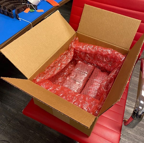 An example of properly packaged PCBAs.
As we unpack the boards, we do a preliminary inspection without magnification. It is often easy to see large defects such as scratches or component misalignment this way. This initial inspection also helps us get a sense of the overall build quality and any systemic issues that might be related to the PCBA design or component pattern. Misalignment of larger components can also be seen at this stage.
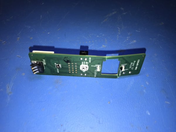
PCBA damaged during shipping. Large defects like this are readily visible in a preliminary unmagnified visual inspection.
Prior to microscope inspection, we can get an overall look of how clean the board is. Even with no-clean flux, it’s sometimes desirable for the board to go through a washing process if the design is amenable to it and subsequent process steps require it. A recent example of this was excessive flux residue covered the test points of some first article boards such that the pins in an FCT test fixture were unable to make good electrical contact. This helped us make suggestions to improve the manufacturing process and our supporting documentation before the board went to larger scale production.
Using microscope magnification, we look at solder joints of both through hole and SMD components. Many problems with solder reflow can be seen visually, particularly with magnification. We can often see if a solder joint is unwetted or cracked, or if there was too much or too little solder applied during the pasting process. Loose solder balls and solder bridges are often more visible in a microscope. We also see floating component defects, where component pins may be misaligned. With packages such as BGA components becoming smaller and more commonly used, being able to get an initial idea of how well they are reflowing is helpful. If we see anything of concern, it may lead us to request a more advanced inspection process, such as x-ray inspection.
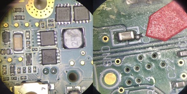
Left: Component floating due to improper solder paste stencil land pattern. Right: Large solder ball, the result of improper solder paste deposition.
Damaged components often stand out, and we also look for damage to the board substrate. When boards are depanelized, cracking can occur near the mousebites or the V-score. Components near the edge, especially ceramic capacitors, can also break. This can help us assess our own component placement, and give us insight on the board house’s depanelization process.
Throughout the process of visual inspection, we can gain insight on the manufacturing process. We also gain insight on our design. As a result of our findings, we may make revisions and refine our supporting documentation. This design for manufacture is a cornerstone of PCBA design at BES.
Sources:
- “Visual Inspection,” Bittelle Electronics Inc, https://www.7pcb.com/Visual-Inspection.php
- “The Why, Where, What, How, and When of Automated X-ray Inspection,” Agilent Technologies white paper, Leinbach G., Oresjo, S., 2001.