.svg "bes-logo (1)")
Modern PCB manufacturing in FR4 provides designers with an incredible range of control, and has become a familiar and ...
Modern PCB manufacturing in FR4 provides designers with an incredible range of control, and has become a familiar and mature technology. However, many applications have mechanical requirements that conflict with the rigid, planar geometry inherent in PCBs. Flexible printed circuits, or “FPCs,” offer an alternative to conventional PCB substrates and allow for a broad range of applications that would otherwise be impossible or impracticable to produce. FPC manufacturing has become common-place, but what are the implications of this substrate for high-speed signal integrity?
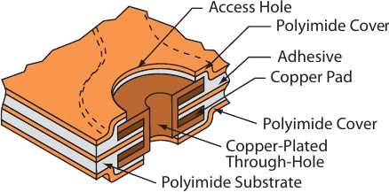
The construction of FPCs is similar to that of PCBs with several notable distinctions. Whereas PCBs are typically built with alternating layers of copper (as the conductor) and fiberglass (as the dielectric), FPCs use a stackup of copper layers, adhesive layers, and polyimide layers. The Polyimide substrate is flexible, and forms the “backbone” of the complete assembly. Compared to the fiberglass used in PCBs, polyimide tends to be thinner and of a lower dielectric value. Of course, as is often the case in electronics manufacturing, a wide variety of materials and thicknesses may be available, dependent on vendors and costs.
FPCs can be constructed with single, double, or multiple layers. This allows a designer to choose from a variety of interconnect structures that are familiar in PCB applications, including microstrip and stripline. Even psuedo co-axial structures can be implemented through the use of vias. FPCs can also be embedded into PCBs, creating “rigid-flex” assemblies. Rigid-flex construction can simplify the mechanical, electrical, and logistic aspects of a design by eliminating connectors, cables, and other physical elements. This reduction in complexity can have profound benefits for reducing manufacturing time and increasing reliability, savings that can dwarf the increased cost of choosing FPC or rigid-flex over conventional PCBs with more electromechanical elements such as cable connectors.
When considering the implications of choosing an FPC substrate instead of a conventional PCB for a given design, the two most important material parameters to observe are typically layer thicknesses and dielectric constant. While the fiberglass composite used in PCBs generally has a dielectric constant in the range of 4.0 – 4.5, the polyimide and adhesive layers of an FPC are more often in the range of 3.2 – 4.0.
In multi-layer PCB applications, a designer is often free to choose the dielectric thickness between layers, with values most commonly between 5 and 50 mil. Extra thickness, if needed, can be added between copper layers to achieve a specified total stack height. However, in FPC applications, thicker layers result in a larger minimum bend radius. Since the dielectric thickness is one of the primary parameters available to control impedance in FPC interconnects, mechanical design motivations can be at odds with electrical design motivations.
In order to better understand these trade-offs, a 2D field solver can be used to simulate the impedance of these structures. Consider a microstrip interconnect implemented on either 2-layers of a multilayer PCB or both layers of a 2-sided FPC. The FPC will have a lower dielectric constant for its adhesive and polyimide layers (assume 3.2), so in order to maintain a constant impedance it would need to A) increase trace width, B) decrease dielectric thickness, or C) decrease trace thickness, compared to a PCB, if all other parameters remain constant. Adjusting the trace thickness is often unfeasible (due to manufacturing constraints and bend-radius limitations), and adjusting dielectric thickness has implications for bend-radius as well. Trace width is likely to be the primary means of controlling impedance, when dealing with strict mechanical requirements for minimum bend-radius. With these factors in mind, we should expect to see a lower impedance for the same microstrip structure implemented with typical PCB and FPC substrates.
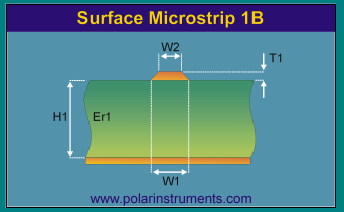 Figure 2: Microscrip simulation model
The parameters of these structures can be simulated in a tool such as QUCS or Polar Instruments' SI9000. The values listed in Table 1 were used to establish the test.
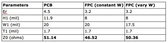 Table 1: Microstrip Impedance Simulation Parameters
The values chosen for this simulation reflect standard and lowest cost parameters available from Sunstone Circuits (despite the significant change in stack-up height between the PCB and FPC models, the impedance change is relatively small. Adjusting the trace-width by 12.5% brings the impedance back to an acceptable approximation of a typical 50 ohm transmission line. In this example we can see that the FPC's smaller dielectric constant is somewhat balanced by its thinner dielectric thickness. This is a convenient combination of parameters and can allow for similar trace sizing in both FPCs and PCBs.
One situation in which trace width may differ from PCBs in FPC applications is the establishment of “bending zones.” Manufacturers often recommend that sections of FPCs intended to permanently or repeatedly bend should have an increased trace thickness, to provide mechanical support for the structure. Although there is mechanical motivation for this design feature, increasing trace width will lower the impedance of the interconnect, and the resulting impedance discontinuity will lead to reflections. Once again, a 2D field solver can be used to evaluate the significance of this type of discontinuity.
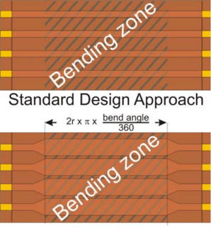
Figure 2: FPC Bending Zone
Image Credit: Flexible Ciruit Technology 3rd Edition, Joseph Fjelstad 2006
The same trace width from the previous simulation was employed for the non-bending section of a hypothetical FPC, and the trace width was doubled for the bending section. This increase in width is conservative relative to some manufacturer recommendations, which may suggest as much as a factor of three increase.
The results of the simulation are listed in Table 2. The increase in trace width results in a reduction of impedance from approximately 50 ohms to 32 ohms. This is a significant discontinuity, and depending on application may result in serious problems.
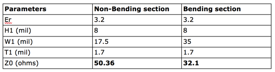 Table 2: Impedance discontinuity from increased trace width in bending sections
If an FPC application requires a small radius bend and there is concern for the mechanical robustness of the design, alternatives to increased trace width should be considered. Higher quality copper foils are available from many manufacturers, with features such as smaller grain size. These more controlled materials can be more resilient to tight bends and repeated flexing. If a permanent bend is required, and the copper layer is intended to undergo plastic deformation so that it will hold its bent shape, wide copper features can be placed adjacent on either side of the impedance controlled traces. This case is an example of the careful balance between mechanical and electrical trade-offs.
One of the most appealing applications of FPC technology is rigid-flex construction, and the interface between the PCB substrate and FPC substrate is an interesting area to consider for its impact on signal integrity.
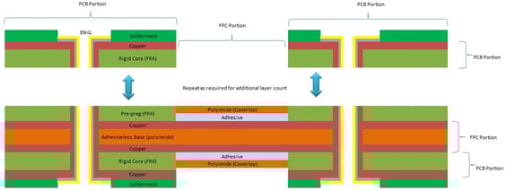 Figure 3: Rigid-flex stackup
A typical rigid-flex assembly uses the same copper and internal polyimide layers of the FPC as internal layers of in the PCB, as shown in Figure 3. However, the external dielectric coating of the FPC is likely to have a different dielectric constant from the FR4 pre-preg in the adjacent PCB region. For a microstrip interconnect, the overall impact of this should be minimal as the dielectric between the trace and its return path remains the same. However, a stripline implementation would see a more significant impact if the dielectric between conducting layers was pre-preg in the PCB region, but polyimide and adhesive in the FPC region. If a stripline architecture was required (for example, to eliminate far-end cross-talk), the dielectric layers between the copper layers of the stripline should be made of materials with constant dielectric properties. Fortunately, many manufacturers can produce multi-layer FPCs that have these properties.
Si9000 was used to evaluate the impedance discontinuity between PCB and FPC regions, looking at microstrip interconnects. The parameters and results of the simulations are contained in Tables 3 and 4.
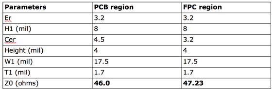 Table 3: Coated Microstrip impedance discontinuity at the PCB-FPC interface
The change in dielectric constant of the material above the microstrip structure has a noticeable impact on the impedance, but depending on the application it may be tolerable at 2.6% variation. For situations where this would not be an acceptable discontinuity, the trace width could be adjusted on either side of the interface to achieve a closer impedance match.
Another common feature of FPCs is the use of hatched planes. Continuous copper pours have a reduced bend radius compared to layers with signal layers made up of smaller traces. Hatching the pours improves flexibility, but leads to a more complex return path for microstrip or stripline interconnects. The impact of this feature varies by application and, like aspects of signal integrity, should be evaluated on the case by case basis, depending on the requirements and margins of a given design. Let's examine the impact of hatching in our hypothetical FPC design.
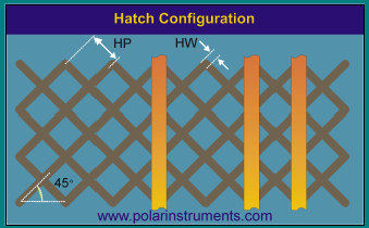 Figure 4: Hatching parameters for FPC planes
Hatching configurations are typically defined by angle, line separation, and line width. For a simulation example, a fill density of 50% is chosen. Removing conductor material from the return path should increase the impedance a signal sees on the microstrip, so we should anticipate a higher impedance. The simulation parameters and results are listed in Table 4.
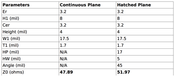 Table 4: Microstrip impedance for hatched and continuous return planes
The overall impact of the hatched plane is manageable, at a difference of approximately 4 ohms - a change of 8.5%. Adjusting the line width to approximately 20 mil would make up for this impedance change. Considering the earlier example of the desire to use wider traces in bend areas, implementing a hatched return plane could be helpful in maintaining desired impedance.
Overall, FPC structures are well suited to high speed interconnects. Eliminating connectors and other mechanical interfaces avoids impedance discontinuity, and in many cases reduces manufacturing costs and improves reliability. Although there are significant differences in the sizes and material properties of FPCs as compared to PCBs, these factors can combine favorably for thin designs and small bend radii.
Some manufacturing recommendations and mechanical requirements (such as widening trace length in bending zones) are at odds with maintaining good signal integrity. Finding the proper balance between these different design motivations requires careful planning and analysis but, when implemented well, FPCs are a compelling and robust technology.